DMG1083 LED Tiles #
| Manufacturer | digiLED |
|---|---|
| Model | DMG1083 |
| Size | 250×250 mm |
| Resolution | 78×78 px |
| Colour depth | 14-bit |
| Pixel pitch | 3.205 mm |
| Supply voltage | 5 V |
| Supply current | ~10 A |
History #
These are video wall tiles which were donated in September 2023. They were part of a batch of tiles which had to be recalled due to an unacceptable failure rate, though we haven’t seen any indication of these failures in testing (it may simply be an issue with colour consistency).
Approximately 800 tiles were received in this batch. We distributed a significant portion of them via the swapshop at EMF 2024.
Description #
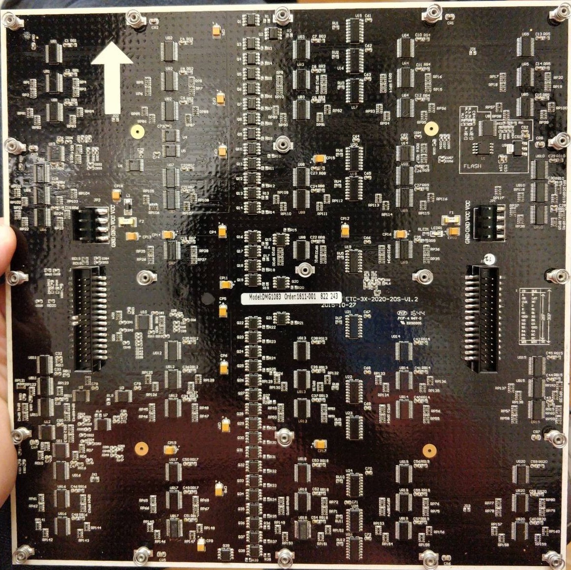
These tiles are originally from a digiLED IMAG-R 3200 screen. They were driven with a Novastar system using the MRV270/MRV470 receiver card, with each receiver driving a module comprising a 2x2 array of tiles.
It appears these LED tiles are similar or identical to models DMG1085 and DMG1075 (perhaps the only difference is the specific model of LEDs).
The PCBs are mounted in a beautifully-manufactured aluminium frame which has magnets and alignment pins for mounting.
Electronically, this as an 80x80 px display with 2 missing columns/rows. The 20 driver chips are capable of driving 320 pixels (4 rows) at a time, which means 6400/320 = 1/20th of the screen is driven at once.
The board also features a MOM (memory-on-module) flash chip (neatly labelled in a box on the silkscreen) which seems likely to contain panel-specific calibration data.
More detailed info on the electronics.
Interface #
Power is provided on a 4-pin JST VH connector:
| 5V |
| 5V |
| GND |
| GND |
Data is on a 2x15 connector:
| CS | SLK |
| A | B |
| OE | LAT |
| CLK | NC |
| C | D |
| E | R1 |
| G1 | B1 |
| GND | R2 |
| G2 | B2 |
| R3 | G3 |
| B3 | GND |
| R4 | G4 |
| B4 | NC |
| SR | NC |
| MSI | MSO |
The CS, SLK, MSI, and MSO lines are likely related to the MOM flash and are not required to drive the display.
The SR line is currently a mystery. The panel appears to work with it disconnected. (Untested hypothesis: could this connect the data lines to the output of the shift register chains to allow the feedback data from the LED drivers to be read back? Perhaps this is what the 74HC4051D ICs are doing.)
The remainder of the pins appear to be a standard “HUB320” interface:
A,B,C,D,Eare address lines.R1..4,B1..4,G1..4are the pixel data lines (which are connected to the input of the MBI5153 shift register drivers).CLK,LATandOEare the standard control lines, but as discussed below, the behaviour is anything but standard. They correspond to theDCLK,LE, andGCLKpins on the MBI5153.
Data line inputs are buffered with 74HC245 bus transceivers. These must be driven with 5V logic levels – 3.3V is not sufficient. The Novastar cards use the 74HCT245 as an output buffer to level-shift 3.3V to 5V. If you use a different level-shifter you should verify that it has a fast enough rise time to handle the required frequency.
The two data connectors on the left and right sides are directly connected and the pinouts are identical. (This is convenient for connecting a logic analyser.)
Driving #
Don’t be deceived: while the interface on this panel looks superficially similar to smaller LED matrix panels, this hides the significant complexity of the MBI5153 driver chip. You’ll need to refer extensively to the MBI5153 datasheet and application note.
The CLK line on the connector feeds DCLK on the MBI5153s.
The OE line on the connector actually feeds the GCLK input on the MBI5153s, and this provides both blanking and the PWM reference clock for the drivers.
The LAT line on the connector feeds the LE input on the MBI5153. This not only handles latching-in the pixel data, but also sending other commands to the MBI5153, depending on how many DCLK pulses are sent while LAT is asserted.
A whole frame’s worth of pixels is clocked into this panel at once, and held in a SRAM double-buffer on the MBI5153 chips. Once this is complete, the output is blanked and a VSYNC command is sent to the MBI5153, which switches the buffers over. The previous frame is displayed while the next frame’s data is being clocked in.
Since there are 20 “scan lines” (320 pixels each) on this screen, this means that the driver chip must switch the scan line data it’s outputting at the same time as the controller switches the scan line address. The MBI5153 does this on the 512th rising edge of the GCLK, so the least significant address line must be clocked at 1/512th the frequency of the GCLK (or 1/256th if the “GCLK multiplier” feature is used).
The MBI5153 has the number of scan lines configured in its configuration registers (among other things). This configuration must be written to the panel before any data is sent. Note that there are 5 address lines but the number of scan lines is 20 so the address lines need to roll over at 0x14.
Example code #
- eta has some working code to drive these panels in Rust using PIO on the Raspberry Pi Pico and gave a talk about this at EMF 2024.
- mrcodetastic’s code for the ESP32S3
Pictures #